[an error occurred while processing this directive]
Device Driver for High-Resolution Clock
Goals
- Learn and understand the fundamentals of writing a device driver.
- Play with real hardware.
- Learn about interrupt handling in L4.
Motivation
The kernel maintains in the kernel information page (KIP) a real-time
clock with a 1ms resolution. For many purposes, e.g., benchmarking, a
higher clock resolution is desired. The U4600 machines feature a chip
which contains several high-frequency counters which can be used for a
timer.
The Driver Interface
Your driver needs to export the interface specified in src/clock.h. There are the
following functions:
- start_timer
- Initialises the driver.
- register_timer
- Registers the calling thread to receive an IPC message after a
specified time interval (in microseconds, though actual wakeup resolution will
depend on the timer resolution). Several registrations may be
pending at any time.
- time_stamp
- Returns the current real-time clock value (microsecond
accurate).
- stop_timer
- Stops operation of the driver. This will cancel any outstanding
timer requests (by sending them a premature IPC indicating
failure).
The IPC message sent by the timer contains in register 0 a return
code (TIMER_R_OK, TIMER_R_UINT, TIMER_R_CNCL)
and in register 1 the present value of the real-time clock.
The U4600
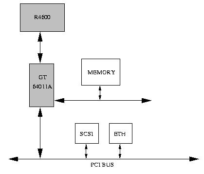 This is a simplified block diagram of the U4600 boards. The GT chip is a PCI
bridge. It acts to interface the CPU with the PCI bus as well as to
memory. Full details of the GT chip can be found its reference manual [1].
This is a simplified block diagram of the U4600 boards. The GT chip is a PCI
bridge. It acts to interface the CPU with the PCI bus as well as to
memory. Full details of the GT chip can be found its reference manual [1].
The R4600 has 8 IRQ exceptions consisting of 2 "software IRQs", 5
external hardware IRQs, and 1 IRQ that can be configured via external
logic to either the internal timer (which it is on the U4600) or another
external IRQ.
GT Chip
Your main job is to learn how to program the GT chip to generate timer
interrupts and how to write an L4 driver to handle these
interrupts.
The GT chip contains four 24 bit timer/counters. For our purposes, we
are only interested in the GT chip as our source of timer
interrupts. You will only be using one of these timers. The GT's
interrupt line is connected to CPU interrupt pin 3 (see
INT_GT64010A in kernel/u4600.h) and
it is clocked at 50Mhz.
There is an abundance of different devices and writing device drivers is
usually seen as a very difficult task. This is true in a sense. However,
programming a device is really just a matter of learning about its
registers, what values to read and write to those registers and when to
do it.
The minimal subset of the GT chip's functionality that you must
understand and use is listed below (the numbers in parentheses are the
offsets of the register addresses from the chip's base address). Refer
to the reference manual for full(er) descriptions [1].
- Internal Space Decode (0x068) : Use this register to
work out where the GT chip is mapped. Hint: you do not need to
actually read or write this register, only need to understand how it
works (you can change this register value if you are keen and
understand what you are doing).
- Timer/Counter[0-3] (0x850-0x85c): The actual
timer/counters. You need to use at least one of them (take your pick).
NOTE: Do not set the timer resolution to higher than 50ms. That
is, pick a timer interval of 50ms or higher. The value you pick here
affects the resolution of the register_timer() interface.
- Timer/Counter Control (0x864) : Enable and disable each
timer as well as determine their operational mode.
- Interrupt Cause (0xc18) : When an interrupt occurs, this
register tells you which of the many sources of interrupts in the GT
chip actually caused it. CPUIntSum (bit 30) is connected to
the R4600 external interrupt pin 3.
- CPU Mask (0xc1c) : This masks the CPU interrupt line.
Again, this is only the minimal understanding that you need. For
deeper understanding, you are encouraged to learn about the other
registers and can even play with those as well.
NOTE: This section is deliberately kept short (e.g., we do not dictated
which timer to use or in what mode to use it in). The idea is that you
work things out for yourself and make your own design and implementation
decisions. There are only two conditions that must be satisfied:
- You must use an interrupt generated from the GT chip.
- You must implement the driver interface described above.
MIPS/L4 Interrupts
The MIPS/L4 kernel exports specific interrupts to a user level interrupt
handler via IPC. A user level thread can register itself to be the
handler for any one of the exported interrupts. After that, any
interrupts of the registered number will get sent as an IPC to the
interrupt handler.
Refer to the MIPS/L4
Reference Manual the MIPS/L4
User Manual for further information on the interrupt registration and
delivery protocol.
NOTE: MIPS/L4 interrupt numbers are one higher than the number of
the actual interrupt pin on the processor. That is, to handle processor
interrupt 0, an L4 handler must register itself for L4 interrupt number
1.
Device Mappings
In MIPS/L4, device registers are memory mapped. That is, hardware
registers can be accessed via normal load/store operations to special
addresses. To access device registers, your handler must first request
the correct device mapping from  .
.
Refer to either the MIPS/L4
Reference Manual the MIPS/L4
User Manual for the device mapping protocol.
Note that all accesses device registers must bypass the
cache. Device mappings sent by use
``uncached'' mappings. If such a device page is mapped on to another
address space, the caching attribute will be maintained (in fact, the
present version of L4/MIPS does not allow changing caching attributes of
mappings). This allows tasks other than initial servers to operate as
device drivers. However, you will be well advised to run your driver
inside the initial server's address space. Later you can migrate it to a
child task, or to a separate initial server (like the serial port
driver).
Endianess
Device frequently use a different byte order than the CPU, so device
drivers must generally deal with endianess, and your clock driver is no
exception. Endianess refers to how indivdual bytes within a multi-byte
word are addressed. The following two figures should illustrate how big
and little endian works. In the figure the numbers refer to the relative
addresses of the individual bytes.
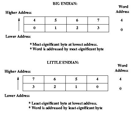
The R4600 is big endian while all GT chip registers are little endian.
Therefore, you will need to do some byte swapping when reading from and
writing to the GT registers.
Issues
You may need to resolve some or all of these issues:
- At what address do the GT chip registers need to be mapped and accessed through?
- Should the timer or counter mode be used?
- What value must be the timer be programmed to to get a frequency of x milliseconds?
- How are the interrupts acknowledged?
- Single or multi-threaded driver?
Files
The file clock.h, as well as some other header files you might
find useful, can be found in src/clock/.
References
[1] GT-64010A Reference Manual.
COMP9242,
School of Computer Science and Engineering,
University of New South Wales
This page is maintained by
gernot@cse.unsw.edu.au.
Last modified: Friday, 11-Aug-2000 15:04:23 AEST
[an error occurred while processing this directive]
Last modified:
Friday, 11-Aug-2000 15:04:23 AEST