Lab 0 - Prep lab, introduction to the Hackster and HW Cryptography
2026-01-10 | Introduction , Hackster , Labs , Cryptography
Introduction
The Prep Lab serves as an essential foundation for the practical aspects of hardware security explored throughout the course. This introductory lab familiarizes students with the Hackster development platform and the tools required to design, implement, and analyze hardware systems. Students will learn to interact with both the ICE40 FPGA and RP2040 microcontroller, establish communication between these components, and explore hardware cryptography in a practical context.
Goals:
- Understand the basics of the Hackster development platform
- Connect the Hackster to your PC
- Develop custom hardware for the ICE40 FPGA to blink an LED and read a button
- Develop custom MicroPython for the RP2040 microcontroller to blink LED/read button
- Design a basic system to pass information between FPGA and microcontroller
- Develop a custom system using I2C to instruct the FPGA to turn on or off an LED when the button on the microcontroller is pressed.
- Use an oscilloscope to capture and examine the signals passing between the microcontroller and FPGA.
- Compile, download, and interact with a hardware cryptography system
- Understand the relationship between the microcontroller-based application and the FPGA-based HW Cryptography functions.
- Use the FPGA to encrypt and decrypt data from the microcontroller application.
- Use an oscilloscope to capture and examine the signals passing between the microcontroller and FPGA.
Deliverables:
None. This preparatory lab is designed to ensure students are comfortable with the tools and techniques that will be used in subsequent labs. It does not include any deliverable components or assessment but is mandatory for progressing in the course.
Note:
Most required software is provided on the CSE Lab machines.
If you cannot get your computer to work during Step 0/1, this is the route.
Step 1: Install Required Software
hackster-programmer repository
Clone the hackster-programmer repository (https://github.com/kiwih/hackster-programmer), this contains required makefiles and example programs.
git clone https://github.com/kiwih/hackster-programmer.git
cd hackster-programmer
Important: do a git pull in this repository regularly (i.e. before each lab), as we often update the code and examples throughout the course!
Using a Lab machine?
First-time setup: We need to install Thonny locally to our account. As we are not administrators, we will install it in a Python virtualenv.
Open one terminal, and run the following: Terminal 2:
cd ~
virtualenv thonny_venv
source thonny_venv/bin/activate
This creates a Python virtual environment called thonny_venv in your home directory, and activates it. You should see that the terminal prompt has changed to indicate that you are now working within the thonny_venv environment, i.e. it sShould now say (thonny_venv) $ at the beginning of the prompt.
Now run
pip install thonny
thonny
This will launch Thonny.
Now open VSCode and open the hackster-programmer repository you cloned earlier. You will edit the code in this repository, and use the integrated terminal to run the makefiles and Thonny to interact with the microcontroller. To make this work, we need to set up the integrated terminal to find oss-cad-suite which is deployed to the UNSW network.
From inside the VSCode terminal, run the following command to source the oss-cad-suite environment:
source /usr/local/share/oss-cad-suite/environment
This should now make it say ⦗OSS CAD Suite⦘ $ at the beginning of the terminal.
You can now proceed to step 2.
On your own machine: OSS-CAD-Suite
- Proceed to https://github.com/YosysHQ/oss-cad-suite-build/releases/tag/2026-01-04 and download the appropriate archive for your OS (e.g., oss-cad-suite-linux-x64…tgz for 64-bit Linux).
- Extract it to a suitable location on your PC.
- (macOS only) Run
xattr -r -d com.apple.quarantine path/to/oss-cad-suiteto disable code-signing warnings. - Navigate to the extracted folder and then source the environment script to set up your environment variables.
For example, on Linux:
cd path/to/oss-cad-suite-build-2026-01-04
source environment
We actually highly recommend that if you are using Windows, you use WSL. Make sure WSL is based on an Ubuntu Linux flavour, then follow the Linux instructions above to download and set up the OSS-CAD-Suite within WSL.
Both Linux and Windows can also download the system using the command line, which is as follows:
wget https://github.com/YosysHQ/oss-cad-suite-build/releases/download/2026-01-04/oss-cad-suite-linux-x64-20260104.tgz
tar -xzvf oss-cad-suite-linux-x64-20260104.tgz # extracts this into oss-cad-suite directory
source oss-cad-suite/environment
You’ll need to source the environment script each time you open a new terminal to work with the Hackster programmer.
On your own machine: THONNY
Thonny is an IDE for Python and (more importantly) MicroPython. We’ll be using it to interact with the RP2040 AppMicro microcontroller.
Install Thonny according to your operating system:
Ubuntu Linux: https://github.com/thonny/thonny/wiki/Linux:
sudo snap install thonny
Note: you need to be a member of the dialout group.
sudo usermod -a -G dialout $USER
Sign in and sign out after doing this.
Windows: (Preferred) Download one of the .exe releases from https://github.com/thonny/thonny/releases, according to the Windows instructions. The current latest version is 4.1.7 (as of 2026-01-25).
Otherwise, if using WSL2, which supports GUI programs, use
sudo apt install python3-tk thonny
OR
sudo snap install thonny
(both are fine)
Mac: Install for Mac using the Github link: https://github.com/thonny/thonny/releases, and install the .pkg file extension. At the time of writing, the latest version is 4.1.7.
Once installed, you can launch Thonny. On Ubuntu, this is as simple as just running thonny in your terminal, in Windows it will be in Start. If using Mac, you can find the Thonny application on Spotlight Search.
Upon opening, if something like this appears, you’re good to go!
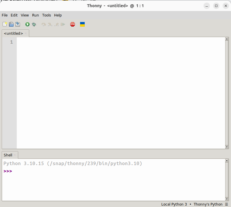
Thonny
(You can ignore any popups for now, just close the program away).
Step 2: Hackster-PC connection
The Hackster platform is connected to your computer using two separate USB-C ports. These USB-C ports are connected to the two RP2040 microcontrollers built into the hackster platform. Each port serves a different purpose.
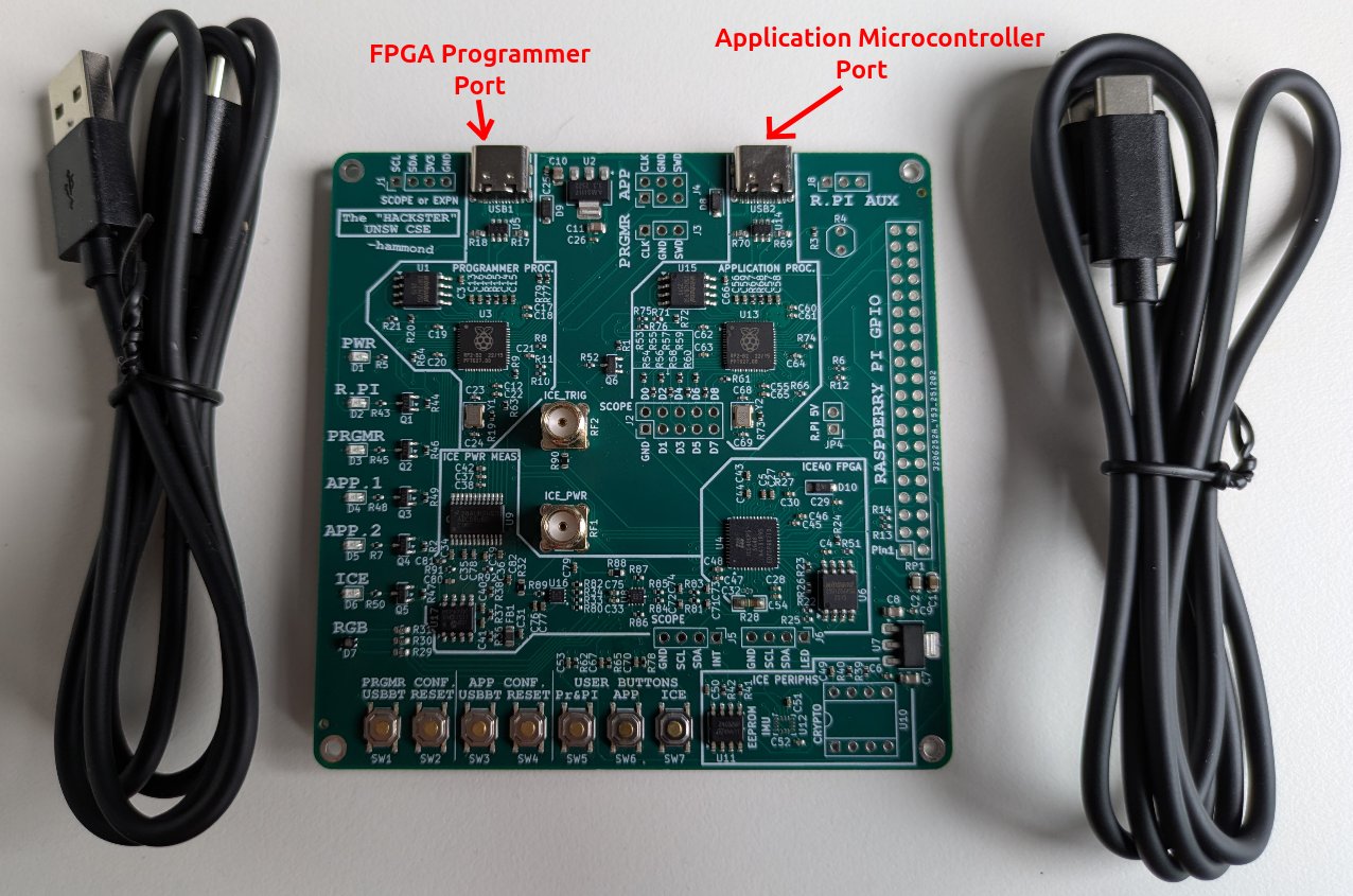
Hackster USB Connections
The left-hand “FPGA Programmer Port” (USB1) is used by the ICE40 FPGA programmer system, hereafter the Programmer. This will need to be connected each time we want to connect to or reprogram the ICE40 FPGA.
The right-hand “Application Microcontroller Port” (USB2) is used by the Application Microcontroller, hereafter AppMicro, which is usually going to be running MicroPython. This will need to be connected each time we want to interact with the AppMicro.
Either port, or both, can be connected at a time and in any order. The Hackster will be fully powered up when either one of the ports is connected.
Now, connect the USB cable from the Programmer Port (USB1) to a free USB port on your computer. Wait for the power LED to come on, then proceed to the appropriate operating system:
Linux
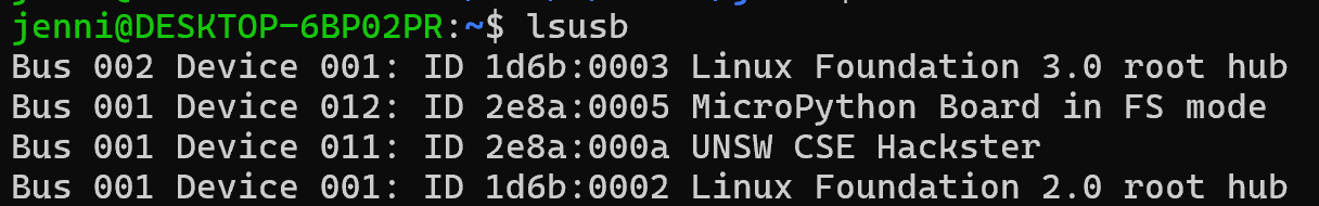
On the lab machines, the Hackster should automatically connect. You can check this by running lsusb. You should see a device called “Hackster”. If connected first, it will be set to /dev/ttyACM0. If you connect the second port, it will be set to /dev/ttyACM1. Once both devices are connected, proceed to Step 3.
Otherwise, On your own machine:
In Linux, you can find the device through:
sudo dmesg
Look for something like the following:

Ubuntu dmesg output after Hackster is connected
This tells us the Hackster FPGA programmer has been registered at /dev/ttyACM0 on this PC.
You can now connect the other USB cable. If you do, and re-run dmesg, you should see something like this:

Ubuntu dmesg output after both Hackster ports are connected
Mac
After connecting the first USB cable, open Terminal and run:
ls /dev/cu.*
You should see something like:
/dev/cu.usbmodem1301
This is the serial port for the Hackster FPGA programmer.
You can now connect the other USB cable. If you do, and re-run the ls command, you should see another port. This is the serial port for the Hackster AppMicro.
In some scenarios, the port you plug in second may fail to connect. So far we have seen this when connecting via. USB C-to-C cables on Mac hardware (A-to-C works fine). To make it connect, you can try:
- Resetting the failing port using the
RESETbuttons; you may need to press them more than once, and holding them briefly may help. - If one port is being stubborn, you can try plugging it in first and resetting the other one.
- Re-flashing the RP2040 may work more reliably than resetting; see the appendix for instructions.
Windows (WSL)
If running using WSL on Windows, USB devices won’t automatically attach to the Linux file system. To allow the serial device to attach, first install usbipd.
The device will have to be reattached whenever disconnected and reconnected (check devices are attached if having connection issues), and can only be active in one file system at a time, not both.
Once usbipd is installed, in powershell, running as an administrator:
usbipd list
This lists connected usb devices, either port will appear in the list of connected devices as:
<busid> <vid>:<pid> USB Serial Device (COM<X>) <state>
Take note of the identity for the first port (the Programmer port), then attach the second cable and re-run usbipd list to see the second device.
For example, see the next figure after both ports are connected:
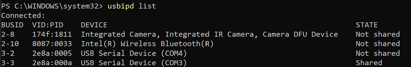
Windows usbipd list output after both Hackster cables are connected (your STATE might differ)
You can now bind and attach the ports to the Linux filesystem for each required port on the Hackster:
usbipd bind --busid <busid>

usbipd attach --wsl --busid <busid>
After running the bind command, the device state will change to “shared”, and after running the attach command, it will change to “attached”.
Now the devices should be visible to WSL. With the devices attached, dmesg, the devices should appear like in the Linux instructions - as Hackster and Micropython entries. In the below screenshot, the FPGA programmer is at /dev/ttyACM1, and Microcontroller at /dev/ttyACM0. Additionally, if listing devices with lsusb, the hardware id (vid:pid) should match those from usbipd.
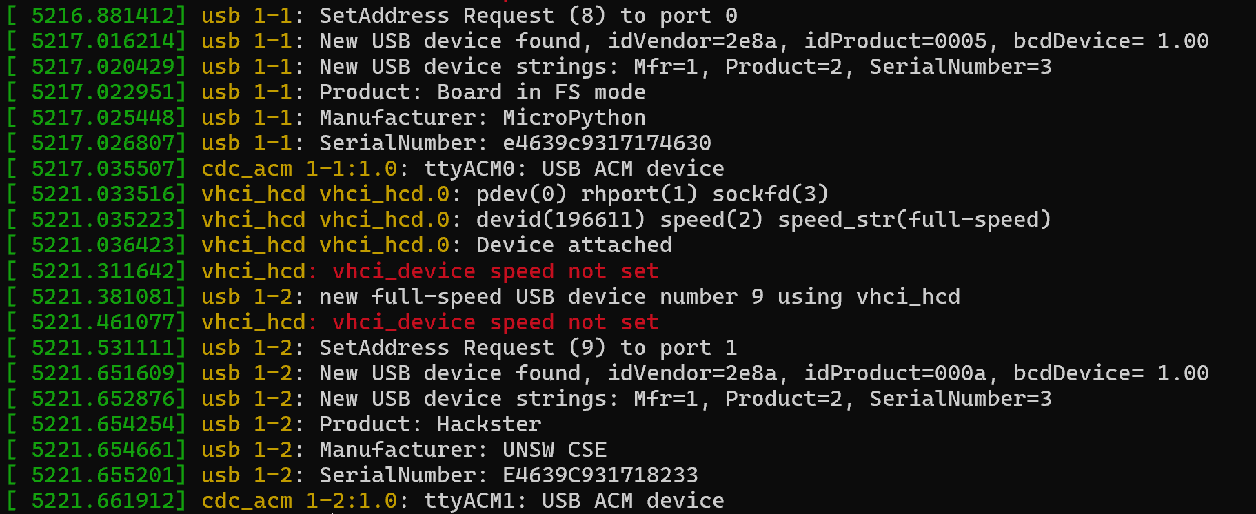
WSL dmesg output after both Hackster cables are connected and attached
WSL lsusb output after both Hackster cables are connected and attached
Step 3: Writing MicroPython to blink an LED from the “application microcontroller” AppMicro RP2040
Make sure you know the port for the AppMicro from Step 2. (If you don’t, go back to that section and do it again).
In my case, on Ubuntu Linux, the port is /dev/ttyACM1. On a MacOS run, the port was /dev/cu.usbmodem1301.
Now, open Thonny. In the bottom right hand corner, select MicroPython (Raspberry Pi Pico) at your correct port (ignore the other options).

Thonny MicroPython Language Selection
In the Shell pane at the bottom, you should get a MicroPython comment. Try a:
print("hello world")
You should see “hello world” printed in the shell.

Thonny MicroPython Print Test
Now we can try blinking the LED!
We can consult the schematic to see what ports are connected.
In our case, the interesting ones are here:
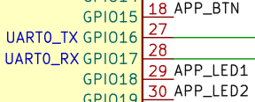
AppMicro LED connection
In the main Thonny window, you can now write a basic program to blink the two LEDs. This uses normal Python syntax, although the language environment is actually MicroPython.
import machine
import time

led1 = machine.Pin(18 , machine.Pin.OUT)
led2 = machine.Pin(19, machine.Pin.OUT)

while True:
   led1.value(1)
   led2.value(0)
   time.sleep(1)
   led1.value(0)
   led2.value(1)
   time.sleep(1)
After typing this into Thonny, you can make it run by pressing the green “play” button.

Thonny Play Button
You should now see the APP 1 and APP 2 LEDs blinking alternately on the PCB. To stop the program at any time, you can press the red “stop” button.

Thonny Stop Button
Sometimes when you try to run a program, it will fail because another program is running. If that happens, just press the “stop” button until you get a new >>> prompt in the shell window.
Suggested Exercises for Step 3
- Make a program which reads from the APP button. If the button is pressed, toggle the change between APP 1 and APP 2.
Further resources for MicroPython:
You can find more information on the MicroPython environment here:
- The full SDK: https://datasheets.raspberrypi.com/pico/raspberry-pi-pico-python-sdk.pdf
- Quick reference: https://docs.micropython.org/en/latest/rp2/quickref.html
- RP2 specific functions: https://docs.micropython.org/en/latest/library/rp2.html
Step 4: Writing Verilog to blink an LED from the FPGA
First, let us examine the target. We are using the ICE40 FPGA, which will allow us to emulate hardware circuits in situ.
When we look at the circuit diagrams we can identify the two signals we will need. The first is the clock input, which will advance the circuit on each transition. This is called ICE_CLK and is connected to pin 37 of the ICE40 FPGA.
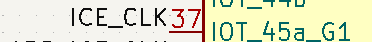
FPGA clock connection
We can also find the LED output, which is helpfully at pin 38.
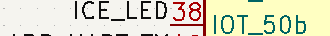
FPGA LED connection
Let us now open the hackster programs repository. Within it, it has the /diy folder, which contains a project “empty-project”. Copy that directory to a new folder “blinky”, then have a look at the top.pcf file.
You should be able to identify the lines which represent the clock and the LED:
# -------------------------- SYSTEM CLOCK ------------------------------------
set_io ICE_CLK 37
set_frequency ICE_CLK 10

# ------------ LED ------------------------------------------------------
set_io ICE_LED 38
(there are other lines too, but we can ignore those for now).
Now, go to the copied top.v file. It is currently empty, so let’s make sure we input the clock and output the LED.
`default_nettype none

// start your project from here.
module top (
   input wire ICE_CLK,
   output wire ICE_LED
);
The input clk is 10 MHz. Let us make the output LED toggle every 1 second.
To do this, we need to divide the input clock by 10,000,000, so we will need a counter which can count to this value.
As log2(10,000,000) ~= 23.3, we’ll need 24 bits to store this counter.
Then, each time the counter reaches 10,000,000 we’ll toggle a register, and that register can drive the LED!
`default_nettype none

// start your project from here.
module top (
   input wire ICE_CLK,
   output wire ICE_LED
);

//the input clock is 10MHz
//we want the output led to toggle every second (1Hz)
//so we need to divide the input clock by 10_000_000
//log2(10_000_000) = ~23.253 = 24 bits

reg [23:0] counter_10MHz_div;
reg toggle_1Hz = 0;
always @(posedge ICE_CLK) begin
   if(counter_10MHz_div == 24'd9_999_999) begin
       counter_10MHz_div <= 0;
       toggle_1Hz <= ~toggle_1Hz;
   end else begin
       counter_10MHz_div <= counter_10MHz_div + 1;
   end
end

assign ICE_LED = toggle_1Hz;

endmodule
This now completes the Verilog code.
After saving this file as top.v, we can now download this code to the board by, in the terminal, running:
make run_fpga FPGA_PORT=/dev/ttyACM0
Note: Your computer may not be using /dev/ttyACM0 for the FPGA! If you’re not sure which FPGA_PORT your programmer is, please read/complete Step 2 again!
This will print a lot of text as it firstly uses Yosys to synthesize your design, then secondly downloads it to the Hackster’s FPGA, verifies it downloaded correctly, and then starts the FGPA. You should see, eventually:
Verification successful. Programming finished.
Starting the FPGA.
If you don’t, please ask your tutor for help!
If you do, great! Take a look at the Hackster board - the ICE LED should now be blinking!
Suggested Exercises for Step 4
- Change the frequency of the blinking LED to 2 seconds, then to 0.5 seconds.
- Read the button input ICE_BTN. Use it to prevent the LED counter from advancing to “freeze” the LED state.
- Examine the
/examples/rgb_demoVerilog, then download it to your FPGA by runningmake run_fpgain the example directory. See how the colors change over time. In the Verilog, examine how a state machine is implemented to advance between colors by changing a maximum counter value for each RGB channel. These channels are connected to a SB_RGBA_DRV primitive, which allows us to use special in-built hardware within the FPGA chip itself - this primitive is designed to run RGB leds through PWM.- After copying
/examples/rgb_demoto your own project directory,- Change the order at which the colors advance
- Change it so that the RGB fades to black between each color
- Change the speed at which the colors change
- After copying
Step 5: Observing the FPGA’s blinking LED with an oscilloscope
Now, let’s observe the blinking LED signal with an oscilloscope.
The Hackster board exposes a number of pins which can be used to connect to an oscilloscope. For the basic LED, we have the option of connecting to the SMA connector RF2, also labelled “ICE_TRIG”, which is directly connected to the FPGA LED output.
(We call it “ICE_TRIG” because we will use this LED as a trigger signal for various measurements in later labs).
This port is found here on the board:

FPGA SMA connection for oscilloscope
To connect to this port, we can use a SMA to BNC cable. Collect yours now and connect it to the ICE_TRIG port.

Connecting oscilloscope probe to FPGA SMA port
Then, connect the other end to a free channel on your oscilloscope.

Connecting oscilloscope probe to oscilloscope
After connecting it, open up the channel’s configuration and make sure it is set to DC coupled, that the probe is set to 1x. (You get to this menu by tapping the channel button for the channel you connected to, then tapping the “probe” button).
Then, change the horizontal and vertical scale knobs until you can see a clear square wave on the screen. (Talk to your Tutor if you’re having trouble with this).
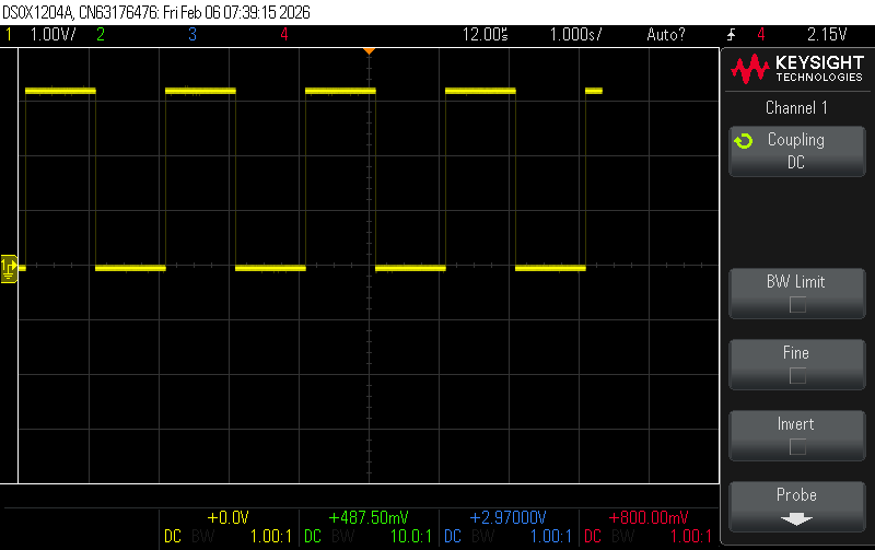
Oscilloscope capture of FPGA LED signal
Just from reading the oscilloscope, we can see that the signal is blinking at a frequency of 0.5Hz, which matches our code which toggled the LED every 1 second (i.e. a full on-off cycle every 2 seconds).
We can also confirm this by pressing the “measure” button on the oscilloscope, and setting it to measure frequency. Here I measure the frequency and also the Pk-Pk voltage of channel (1), which is the channel I connected to the FPGA LED signal.

Oscilloscope measurement of FPGA LED signal frequency
Suggested Exercises for Step 5
- Change the frequency of the blinking LED in your Verilog code, then observe the new frequency on the oscilloscope. Can you get it to 10Hz? 100Hz? 1kHz?
- Change the duty cycle of the blinking LED (i.e. the proportion of time it is on vs off) in your Verilog code, then observe the new duty cycle on the oscilloscope. Can you get it to 25%? 75%?
Step 6: Interfacing the FPGA and AppMicro together with GPIO
Let us now look at the block diagram for the Hackster board.
This is essentially a simplified schematic which describes how the four major components on the board are connected together:

Hackster complete system diagram
As we can see, there are plenty of different connections between the different components!
We’re going to be looking at interfacing the AppMicro (the green box on the left) with the ICE40 FPGA (blue box middle bottom).
The primary options for the connectivity are covered by the links which start on the AppMicro as GPIO (9 wire), UART1, and I2C0.
For the first part of this walkthrough, we will use the GPIO.
In the /diy folder, create a new directory called “gpio_for_rp2040”.
Then, copy in your top.v, top.pcf and Makefile from the blinky project.
We will need to edit the top.pcf file first. Here we split the AppMicro signals into inputs and outputs:
top.pcf:
# --------------------------------------------------
#- hackster constraint file for gpio_for_rp2040 demo
#- By Hammond Pearce
#- August 2024
#- MIT license
# --------------------------------------------------

# ------------- SYSTEM CLOCK -----------------------
set_io ICE_CLK 37
set_frequency ICE_CLK 10

# ------------ LED ---------------------------------
set_io ICE_LED 38
set_io RGB_B 39
set_io RGB_G 40
set_io RGB_R 41

# ------------ BTN ---------------------------------
set_io PI_ICE_BTN 6

# ------------ APP_ICE40 comms ---------------------
set_io APP_out[7] 25
set_io APP_out[6] 27
set_io APP_out[5] 26
set_io APP_out[4] 28
set_io APP_in[3] 31
set_io APP_in[2] 32
set_io APP_in[1] 34
set_io APP_in[0] 36
(You can delete the rest of the file for this example)
We now overwrite top.v with these very simple passthroughs:
`default_nettype none

module gpio_for_rp2040 (
   input wire ICE_CLK,
   input wire [3:0] APP_in,
   output wire [7:4] APP_out,
   output wire ICE_LED, RGB_R, RGB_G, RGB_B
);

   assign RGB_R = APP_in[0];
   assign RGB_G = APP_in[1];
   assign RGB_B = APP_in[2];
   assign ICE_LED = APP_in[3];

   assign APP_out[7:4] = 4'b1111;
endmodule
You should now rename this file as gpio_for_rp2040.v.
Now, update the Makefile to change
SYNTH_SOURCES = gpio_for_rp2040.v
and
SYNTH_TOP_MODULE = gpio_for_rp2040
This creates a simple design where the RGB LED and LED output are directly wired to the signals coming from the AppMicro.
You should now be able to run make run_fpga, and once you have done this, this simple design will be loaded to the FPGA, with no visible outputs (yet).
We now need to make it so that these LEDs are emitted. We do this in Thonny. Open up a new program window (re-visit Section 4 if you are not sure how to do this).
Then, create the following simple program:
import machine
import time

app0 = machine.Pin(6, machine.Pin.OUT) #signals to FPGA
app1 = machine.Pin(7, machine.Pin.OUT)
app2 = machine.Pin(8, machine.Pin.OUT)
app3 = machine.Pin(9, machine.Pin.OUT)

led1 = machine.Pin(18, machine.Pin.OUT) #signals to RP2040 LEDs
led2 = machine.Pin(19, machine.Pin.OUT)

app0.value(1) #the ICE40 rgb leds are active low
app1.value(1) # by setting each of these to 1
app2.value(1) # we are actually turning them off

app3.value(0) # the ICE normal led is active high

while True:
  app0.value(0)
  led1.value(1)
  led2.value(0)
  time.sleep(1)
  app0.value(1)
  led1.value(0)
  led2.value(1)
  time.sleep(1)
As with before, when running this the APP LEDs will blink alternately.
Now, however, the ICE RGB LED should be blinking blue in time with “APP 1” LED!
This is because the RP2040 is now emitting the signal APP0, which is being read in by the ICE FPGA and forwarded to the appropriate signal.
Suggested Exercises for Step 6
- Make the FPGA’s RGB LED blink different colors by passing through signals from the AppMicro.
- Make a program which reads from the ICE button and passes the signal to the AppMicro. If the button is pressed, toggle the output in the AppMicro between LEDs APP 1 and APP 2.
- Extend your answer from 2 to make the FPGA’s output a toggle based on the button presses (i.e. toggles on when the button is pressed, stays on until the button is pressed again, when it toggles off). Use this toggling behaviour to control a state machine in the AppMicro to advance a color signal which is then returned to the FPGA to display on the RGB LED.
Step 7: Recording GPIO interface signals with an oscilloscope
Starting from the code from Step 6, update the MicroPython for the AppMicro to feature
time.sleep(0.001)
Instead of the previous “1”s.
Now, when you run the program on the FPGA bitstream from Step 5, the LED will blink too quickly to see. Instead, it will appear constantly on (and a bit dimmer than usual). However, you know that you are actually turning the signal on and off as this is how the code worked from earlier: we are just having a very short delay between the on and the off signal.
Let’s observe that this is indeed the case. On your hackster board, plug in two male-to-female wires to the SCOPE pins at J2, one going to GND and one going to D0 as shown in the following photo:
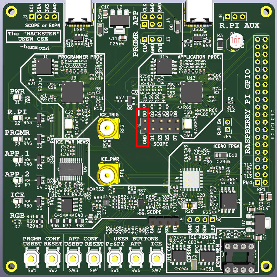
Connecting oscilloscope probes to the FPGA board
And in the following photo:

Connecting oscilloscope probes to the FPGA board
Once these two wires are connected, connect them to your oscilloscope probe, with your D0 wire going to the probe signal, and the GND wire going to your scope probe’s ground lead (the outer wire/crocodile clip).
You may now need to change the channel settings on your oscilloscope to the channel you connected to, and set it to DC coupled. If your probe is set to 10x on the physical probe, make sure to set it to 10x in the oscilloscope settings too (or set it to 1x on the probe and in the settings).
Now, configure your oscilloscope until you can see a square wave on your screen. This may involve manipulation of the Horizontal and Vertical capture knobs, as well as the use of the “Trigger” knob to set up the capture. (Talk to your Tutor if you’re having trouble with this).
Eventually, you should have something like this:
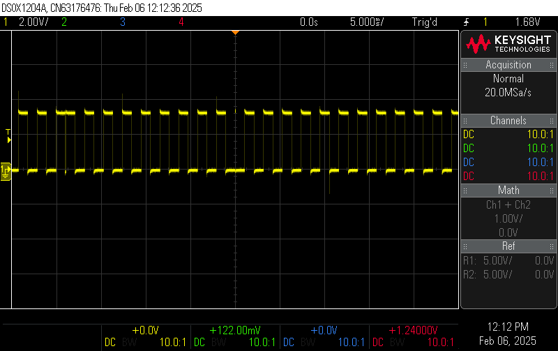
Oscilloscope capture of the FPGA GPIO signal
(Note also the glitches! Why do you think these might be occurring?)
We can now use the oscilloscope to measure the frequency of this signal. Press the “Meas” (measure) button, and then select it to measure Frequency. Once you’ve set it up correctly, it should look something like this:
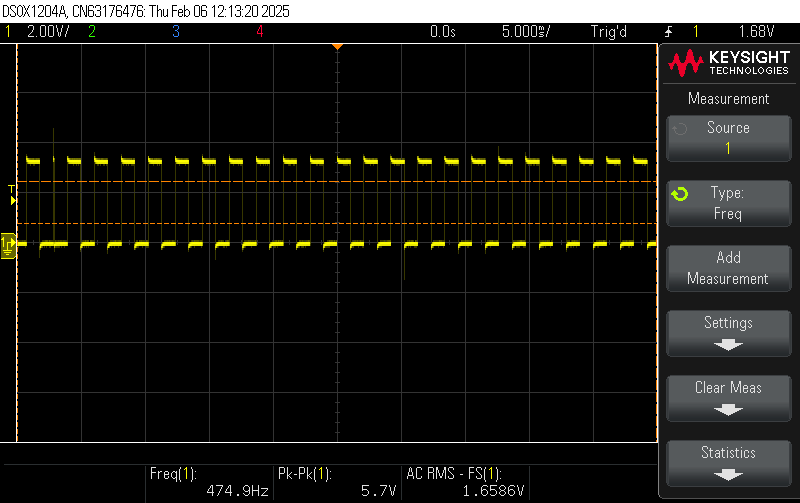
Oscilloscope measurement of the FPGA GPIO signal frequency
Here we can see a captured frequency of 474.9Hz, but it is not stable - occasionally it will jump to nearly 1kHz! We can speed this up more. Let’s comment out the time.sleep commands altogether so they become
# time.sleep(0.001)
Then, run the MicroPython program again, and record the new frequency. It should now be much faster! For example,

Oscilloscope measurement of the FPGA GPIO signal frequency with no delay
Here the capture shows nearly 20kHz.
Suggested Exercises for Step 7
- Explore changing the MicroPython code to achieve desired frequency outputs. What is the fastest frequency you can obtain?
- Explore using two inputs and custom triggers. Can you get the Oscilloscope to launch a capture of Channel 1’s square wave by having an impulse delivered to Channel 2 which was in turn created by an FPGA button press?
Step 8: Interfacing the FPGA and AppMicro with SPI
Up to this point in the prep lab we have just been using simple GPIO signals to communicate between the FPGA and the AppMicro. Such methods do not scale very well. It is better to use a communication protocol based on serial data. Here, a single wire will carry bits of data which vary over time. A number of different serial protocols exist, including UART, SPI, I2C, and USB, and more complex protocols may have multiple data lines (e.g. USB3, ethernet, AXI, Wishbone, DVI, etc.). In this part of the lab we will use a protocol called SPI (Serial Peripheral Interface).
SPI is a widely used synchronous serial communication protocol designed for short-distance communication, primarily in embedded systems. It enables fast, full-duplex data exchange between a main device (e.g., a microcontroller) and one or more secondary (peripheral) devices (e.g., sensors, memory chips, or displays) (other nomenclature calls this as “master” and “slave” devices).
Key Features of SPI:
- Four-wire interface: Typically consists of:
- MOSI (Main/Master Out, Secondary/Slave In),
- MISO (Main/Master In, Secondary/Slave Out),
- SCK (Serial Clock),
- and SS (Secondary/Slave Select).
- Full-duplex communication: Data can be sent and received simultaneously.
- Relatively high-speed operation: Suitable for applications requiring rapid data transfer.
- Multiple slave support: Uses individual SS lines or a daisy-chain configuration to communicate with multiple devices.
SPI can be thought of as two linked “shift registers”, as per the following image:

SPI as linked shift registers
It works as follows. Two registers, one in the master, and one in the slave, are linked via MOSI and MISO when the SS line is activated. The MOSI connects the output of the master to the input of the slave; and the MISO connects the input of the master to the output of the slave. Then, with each clock cycle on SCK, one bit of the shift registers are exchanged in a loop.
On the hackster board, we can implement an SPI between the AppMicro and the ICE40 FPGA. We can do this in the 9 unspecified GPIO between the two devices. One such example doing so is presented for you under the examples/spi_simple directory of the hackster-programmer repository.
First, examine the Verilog code in spi_simple_top.v. Observe that we are not using the ICE_CLK input, instead we are clocking the whole circuit with the SPI SCK input (this simplifies matters).
There are two possible options when this circuit runs. If NORM_CS_N is “1”, the shift register takes the value at data_in (which is the value at data_out with the MSB replaced with the button). If NORM_CS_N is “0”, the shift register will instead capture one bit from MOSI and release one bit to MISO (via a temporary register which is needed to account for SPI sample capture delay).
Run make run_fpga to deploy this design to the hackster. Now examine the code spi_simple.py, which is a MicroPython program ready to run on the AppMicro.
Here, we can see that the MicroPython creates an SPI (with a relatively low baud rate), then creates two one-byte buffers, one called txdata and one called rxdata. These will be used when exchanging the data via the SPI (data sent from txdata and received into rxdata).
In each iteration of the while loop, we will engage the SPI by setting the NORM_CS_N value to “0”, then running spi.write_readinto(). After we’ve exchanged the bytes, we reset the NORM_CS_N value to “1”, then have a very short delay, before running one more SCK clock cycle. In this way we will perform both functions encoded in the Verilog - we will do one complete byte transfer of SPI, and we will do one button capture.
In Thonny, create a new tab and copy in the program. then run it. You should see the RGB LED turn blue due to the transmission of the 0x08 value from the AppMicro. In the shell of Thonny you can also see we are receiving back the transmitted byte (as the bottom seven bits are retained).
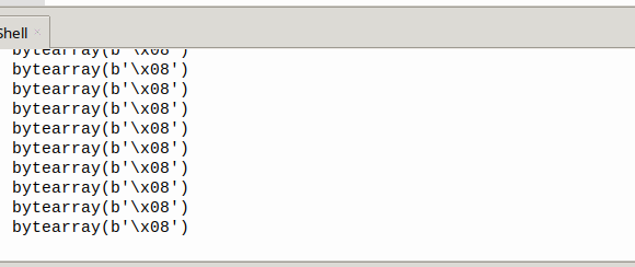
Thonny SPI output
Meanwhile, you can press the ICE button and on the FPGA and observe the value change!

Thonny SPI output during a button press
The hexadecimal value now reads “88” as we have replaced the MSB with a “1” from the button, and binary 1,0,0,0,1,0,0,0 is 0x88.
Suggested Exercises for Step 8
- Explore changing the MicroPython code to mask off the received top-level bit and print “button pressed!” or “button released!” upon a change in the received value.
- Change the Verilog and MicroPython to support multi-byte transmissions. Make a counter which increments with button presses, and return the value of the counter over the SPI.
Step 9: Recording SPI signals with an oscilloscope
Now, let’s observe the SPI signals on the oscilloscope. First, set up the project according to Step 8.
Now, as with Step 7, we’re going to connect up the Hackster to the oscilloscope. This time we have a few more wires to investigate. The relevant pins are as follows:
D0 - SCK
D2 - MOSI
D3 - MISO
D4 - NORM_CS_N

Hackster SPI pin connections for oscilloscope
For now, use just two probes.
Connect the first one, on channel 1, to once again be connected to the GND and the D0 (SCK). You can then connect channel 2 to D2 (MOSI).
Once connected, configure your scope so that the SCK is at the center of the screen and MOSI (D2) is placed above it.
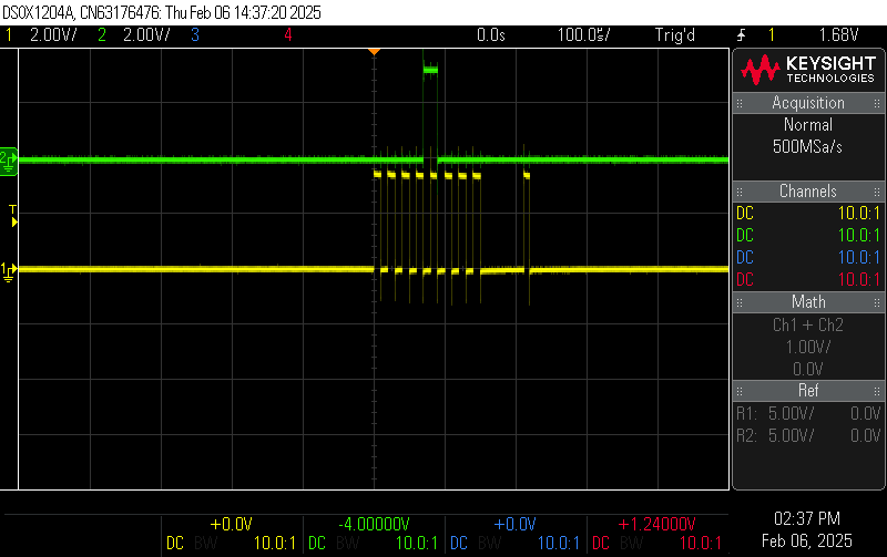
Oscilloscope capture of SPI SCK and MOSI signals
This is what two of the four signals look like when we’re reading SPI! (Also observe the last clock cycle on SCK, which is not part of the SPI protocol, but is how we engage the button load for our particular hardware design).
Now, on the oscilloscope, press “Analyze” to go into the analysis mode. Select “Serial” under “Features”, then “SPI” under “Mode”, then under the “Signals” menu set “Clock” to channel 1 and “MOSI” to channel 2. You may have to re-select Features to enable Serial (the box will color in), then the oscilloscope will display the captured values like so:
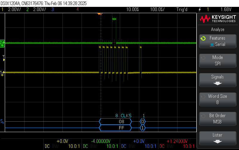
Oscilloscope SPI analysis mode showing decoded data
This is successfully reading the hexadecimal value 0x08 being transferred over SPI to the FPGA from the AppMicro!
We can now transfer the wire from D2 to D3, and then also switch the channel 2 from MOSI to MISO.
Now, we’re observing the response from the FPGA on the MISO line. By default it will return 0x08.

Oscilloscope SPI analysis mode showing decoded data on MISO
Now press the button on the ICE FPGA and observe how you capture 0x88 instead of 0x08!

Oscilloscope SPI analysis mode showing decoded data on MISO during button press
Suggested Exercises for Step 9
- Repeat these exercises using your expanded code from Step 8.
- Pair up with a friend to get a third and fourth oscilloscope probe, and capture MISO, MOSI, SS and the SCK all at once.
Step 10: Implementing and inspecting a full Hardware Cryptography system on the Hackster platform
The examples/ directory also includes two projects, spi_des and spi_aes.
These implement a DES cryptography core and an AES cryptography core, respectively. Each core is connected to an SPI peripheral to enable communication with the AppMicro, as well as clocking the core more generally (in these two demos, the AppMicro clocks the FPGA rather than the programmer).
They are connected as follows:
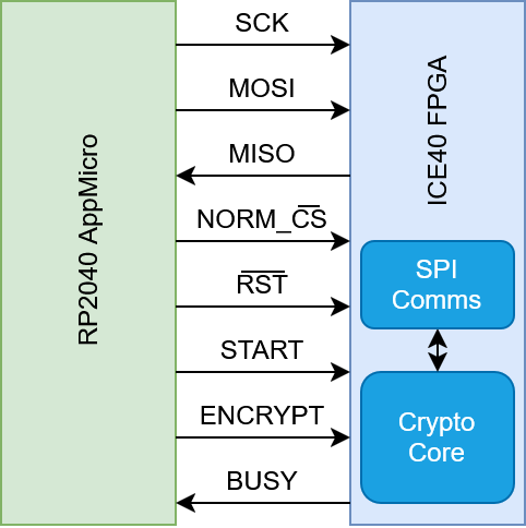
System diagram for the SPI DES and AES examples
It is now your task to download and run these examples, doing your best to understand how it is that they work and communicate.
You will be given some additional support via the Week 2 lecture (Cryptography in Hardware).
Note that each example does include the MicroPython code which implements the SPI handling.
Suggested Exercises for Step 10
- Pair up with a friend to get a third and fourth oscilloscope probe, and explore the different signals you can capture on the scoping pins.
- Implement or find a library for AES and DES in MicroPython and benchmark how long the AppMicro takes to run the equivalent code - is it faster or slower? Your result may surprise you!
- (The FPGA has a much lower than normal clock rate in this system - is it too slow?)
- [Extra for experts] Try modifying the ICE40 implementation so that the entire system does not depend upon SCK as the input clock and instead uses the standard 10MHz ICE_CLOCK from the programmer. Now which is faster?
Conclusion
In this lab, you have been introduced to the CSE Hackster board, and have learned how to write code for both the AppMicro RP2040 microcontroller and the ICE40 FPGA. You have also learned how to use an oscilloscope to observe signals from the board, and have observed a full hardware cryptography system on the platform.
These skills will be essential for the rest of the course, and you will be building on them in the next labs.
Appendix: Re-flashing the firmware on the Hackster
Programmer Firmware:
- While the Programmer is connected to the computer, press and hold the PRGMR USBBT button SW1 then tap the PRGMR RESET button SW2. Then, release the PRGMR USBBT button.
- A “USB device” will appear on your computer.
- Drag and drop the
cse-hackster-fw-2026-feb.uf2from the firmware/ directory of the hackster-programmer repository to the new device. - The Hackster will reboot and the firmware is now installed.
AppMicro MicroPython Firmware:
- While the AppMicro is connected to the computer, press and hold the APP USBBT button SW3 then tap the APP RESET button SW4. Then, release the APP USBBT button.
- A “USB device” will appear on your computer.
- Drag and drop the
micropython-RPI_PICO-20251209-v1.27.0.uf2from the firmware/ directory of the hackster-programmer repository to the new device. - The AppMicro will reboot and the firmware is now installed.