COMP6420's Hardware Capture The Flag (CTF)
2026-03-26
Download the CTF sides: COMP6420_2026T1_Week7_CTF.pdf

Situation:
You are a member of the REBEL ALLIANCE, part of a team which has just extracted a data core from a recently downed GALACTIC EMPIRE ship. The data core contains critical information about the EMPIRE’s operations, but it is protected by a SELF-DESTRUCT mechanism which will destroy the core after just THREE MINUTES.
Objective:
Firstly, you need to understand how the data core’s self-destruct mechanism works. Then, you need to design and implement an attack sequence which will allow you to disarm the self-destruct mechanism before the three minute timer expires.
Fortuately, prior attacks on similar data cores have revealed a number of design elements, as shown in the video below:
As depicted, the data core has clearly been built to a reduced budget, consisting of a Raspberry Pi Zero 2 connected to a standard Hackster platform. However, this does not prevent the self-destruct mechanism from being a significant threat, as the data core still has a number of tamper-proofing measures in place:
-
The data core is encased in a tamper-proof shell with six screws which must be removed before the internal components can be accessed.
-
The hackster platform contains a light-dependent resistor (LDR) which will trigger the self-destruct mechanism if the PCB is exposed to light.
-
The crucial data is kept in memory, meaning that if the Raspberry Pi is powered down, the data will be lost regardless of whether the self-destruct mechanism is triggered or not.
-
The self-destruct mechanism is triggered by a countdown timer which starts as soon as the data core is extracted from the ship. It consists of two parts:
- A hardware real-time clock (RTC) which keeps track of the time remaining until self-destruction. This has a two-minute timer which will trigger the self-destruct mechanism if it reaches zero.
- A backup software timer runs on the Raspberry Pi, which also keeps track of the time remaining until self-destruction. This has a three-minute timer which will trigger the self-destruct mechanism if it reaches zero.
- REBEL INTELLIGENCE understands there are additional properties of the timers and their communication busses which may be relevant to your attack. You may be able to obtain these through your own research, perhaps by conducting social engineering on known EMPIRE engineers, or by analyzing the design of the data core and its components.
-
The Raspberry Pi is locked down and can only be accessed via a serial console protected by a password.
- This serial port is connected to the ICE40 FPGA, and by default is routed to unused pins on the Hackster (the U10 socket).
- REBEL INTELLIGENCE believes that this port is intended for in-field device management. It has the following properties:
- The baud rate for the serial console is 115200, with 8 data bits, no parity, and 1 stop bit (115200 8N1).
- You can disarm the self-destruct mechanism by sending the message
disarm pass=XYZwhere XYZ is the correct password. - This password consists of three random digits from 0 to 9. It is scrambled each time the core is armed.
- REBEL INTELLIGENCE wonders if this serial port could be accessible via the AppMicro if routed differently through the FPGA fabric?
-
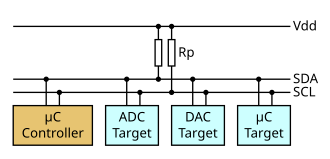
The system diagram for the data core is depicted here:

Data core system diagram
Design Weaknesses?
REBEL INTELLIGENCE believes that these data cores have a number of design weaknesses which may allow you to disarm the self-destruct mechanism before the two and three minute timers expire. For instance, by basing the design on the Hackster platform, the EMPIRE provides additional debug and reconfiguration circuitry which might be exploited to bypass or disable certain tamper-proofing measures.
This is your goal: to identify and exploit these design weaknesses in order to disarm the self-destruct mechanism, so that other members of your team can extract the critical information from the data core. You will need to use your knowledge of hardware security, embedded systems, and reverse engineering to achieve this objective within the given time constraints.
Fortunately, you will be able to design your approach before the ship is ambushed. You will also have access to your own provided Hackster, allowing you to model certain aspects of the data core’s design and test potential attack strategies before you attempt on the live core.
Deliverables and Weightings:
This CTF is worth 30% of your final grade for this course.
- Practical demonstration (15%):
- A three-minute live demonstration of your attack sequence on the data core, showing how you disarm the self-destruct mechanism.
- Report (15%):
- Submit to Moodle a zip containing at least the following files and directories:
/artifacts:/README.md: A markdown file describing the contents of the/artifactsdirectory.- Other files: This directory should contain all artifacts (code, diagrams, etc.) you produced in order to carry out this attack.
report.pdf:- An IEEE two-column conference-formatted report of a maximum of three pages (excluding references).
- Describe your attack sequence, the design weaknesses you exploited, and how you overcame the challenges posed by the data core’s tamper-proofing measures.
- Include recommendations for how the data core could have been improved to prevent your attack (or other attacks in general).
- Discuss also how the EMPIRE could have better secured their data transfer mechanisms, outside the context of the data core itself.
- Submit to Moodle a zip containing at least the following files and directories:
NOTE: HURDLE: YOU MUST SCORE AT LEAST 15/30 MARKS TO PASS THE COURSE
Rubric:
Practical Demonstration (15%)
- Criterion:
- (5%) Delay: Successfully delay the self-destruct mechanism for at least two minutes, allowing sufficient time to access the critical data. Full marks for clever strategies which leverage available design weaknesses to guarantee attack success. Reduced marks for strategies which are more simple or unreliable in nature.
- (5%) Disarm: Successfully disarm the self-destruct mechanism, ensuring that the data core remains intact and the critical information can be extracted. Full marks for clever strategies which leverage available design weaknesses to guarantee attack success. Reduced marks for strategies which are more simple or unreliable in nature.
- (5%) Debrief: Provide a clear and concise explanation / Q&A with the tutor after the demonstration, highlighting the design weaknesses exploited and how the attack was executed.
Report (15%)
- Criterion:
- (5%) (artifacts) Implementation of attack sequence:
- Poor (0-1%): No evidence of the attack sequence or design weaknesses exploited. The
/artifactsdirectory is either missing or contains irrelevant materials, and theREADME.mdfile is absent or provides no useful information. - Good (3%): A reasonable implementation of the attack sequence, with some evidence of the design weaknesses exploited. The
/artifactsdirectory contains relevant code, diagrams, and other materials produced during the attack, but it may be somewhat disorganized or lacking in detail. TheREADME.mdfile provides a basic overview of the contents and how they relate to the attack sequence. The used techniques may be basic and not demonstrate deep understanding of the available attack surface, but they should still be at least partially effective in disarming the self-destruct mechanism. - Excellent (5%): A well-documented and clearly organized
/artifactsdirectory containing all relevant code, diagrams, and other materials produced during the attack. TheREADME.mdfile should provide a clear overview of the contents and how they relate to the attack sequence. The artifacts should demonstrate a clear understanding of the attack strategy and the design weaknesses exploited. To ensure that the artifacts are easy to understand, ensure that you have made good stylistic choices in your code (e.g. meaningful variable names, comments, etc.) and diagrams (e.g. clear labels, legends, etc.). The artifacts should be well-presented and easy to navigate. The artifacts should also demonstrate creativity and originality in the attack strategy, showcasing a deep understanding of the available attack surface and how to exploit it effectively to disarm the self-destruct mechanism.
- Poor (0-1%): No evidence of the attack sequence or design weaknesses exploited. The
- (10%) Written explanation and discussion of the attack:
- Poor (0-2%): Poorly written explanation with little to no discussion of the attack sequence, design weaknesses exploited, or recommendations for improvement. The report may be disorganized, difficult to follow, and may contain numerous grammatical errors. The discussion of how the EMPIRE could have better secured their data transfer mechanisms may be absent or very weak.
- Fair (2-5%): A written explanation is provided, but it may lack clarity or depth. The report may be somewhat disorganized or difficult to follow, and may contain some grammatical errors. The discussion of how the EMPIRE could have better secured their data transfer mechanisms may be present but may lack depth or insight. The report may exceed the page limit or have formatting issues, but it should still be readable and convey the main points of the attack sequence and design weaknesses exploited.
- Good (5-8%): A clear written explanation of the attack is provided, along with links to the artifacts (i.e. screenshots, logs, or other evidence). The explanation should include a discussion of how the attack works and its limitations against a more well-designed defense, while also suggesting ways to achieve that better defense. Does not exceed 3 pages+references and follows the IEEE two-column conference format.
- Excellent (9-10%): A comprehensive and well-written explanation and evidence that clearly describes the attack sequence, the design weaknesses exploited, and the recommendations for improvement. The report should be well-organized, easy to follow, and free of grammatical errors. The discussion of how the EMPIRE could have better secured their data core and data transfer mechanisms should be insightful and demonstrate a deep understanding of hardware and information security principles. The report should adhere to the page limit and formatting requirements.
- (5%) (artifacts) Implementation of attack sequence:
Getting Started:
We will provide several resources, such as this page, which help you begin the process of completing this CTF.
The Hackster schematic is provided on this website, and the bitstream used by the Hackster’s FPGA can be found at /examples/i2c_rpi_passthrough in the hackster-programmer repository on GitHub. You can use these resources to understand the design of the data core and identify potential weaknesses that you can exploit in your attack sequence.
Starting from these provided documents, build up a model of how the device works, and see if you can identify weaknesses.
Good luck, and may the Force be with you!
Appendix: Useful knowledge.
I2C overview
I2C, invented in 1982, is still in wide use today. It is a two wire synchronous protocol with support for multiple controllers and targets (also known as multi-master / multi-slave). Common I2C applications include reading hardware monitors, sensors, real-time clocks, controlling actuators and displays, accessing low-speed DACs and ADCs, etc.
The two wire design of I2C provides a particular strength in that a microcontroller can control a network of devices with just two general-purpose I/O pins and software. Many other bus technologies used in similar applications, such as Serial Peripheral Interface Bus (SPI), require more pins and signals to connect multiple devices.
I2C’s two wires are called “SCL” or “(Serial) Clock”, and “SDA” or “(Serial) Data”. These two wires are connected to all devices in the network bus via an “open drain” configuration, which means any device can either connect the signal to ground (logic 0) or can leave the wire floating (logic 1). The floating wires rise to a positive voltage thanks to connected resistors. We will come back to more details of open-drain in later steps. An example schematic may end up like this:
I2C diagram (Figure reference: https://en.wikipedia.org/wiki/File:I2C_controller-target.svg, CC BY-SA 4.0)
On the Hackster platform there are three distinct I2C buses. The first is called the “Global” I2C, and connects the various controllers (AppMicro, Programmer, and Raspberry Pi) together with the FPGA. The second is called the “Peripheral” I2C and connects two peripherals, an EEPROM and a RTC, to the FPGA. The third is called the “Crypto” I2C and connects the Crypto socket to the FPGA.
A typical I2C transaction looks like the following:

(Image ref: https://www.ti.com/lit/an/sbaa565/sbaa565.pdf?ts=1737448064627 Figure 3-3)
It is made up of a START bit, where SDA falls before SCL, then an 8 bit address frame (with a 7 bit address and a 1 bit read/write flag) which is followed by an ACK from the device matching that address. Then, if it was a read, the target device will emit 8 bits of data while the main device clocks SCL; otherwise the master will emit 8 bits of data while also clocking SCL. Then, the appropriate end sends ACK (master if read, target if write). The data frames will repeat until the master signals a STOP bit by sending SDA high while SCL is also high.
There are three example projects in the hackster-programmer/examples directory relevant to the I2C networks.
The first, i2c_passthru, can be used to bridge the Global I2C bus with one of the other two buses (e.g. to enable the AppMicro to talk to the RTC).
Here, the FPGA simply acts as a pair of bidirectional wires.
The second, i2c_registers, instantiates a basic target/slave peripheral in the FPGA.
The third, i2c_trojan, instantiates both slave and master in the FPGA to act as a hardware trojan.
Tutorial: Learning I2C on the Hackster
Step 1: Bridge I2C communication from application microcontroller to EEPROM
In this step, the FPGA is just acting as “wires”, and you can speak between the AppMicro and the EEPROM. (Make this the RTC?)
Let’s navigate to the examples/i2c_passthru directory.
The file i2c_passthrough.v is the main Verilog module that instantiates two bidirectional I/O pins for SCL and SDA.
We use I/O primitives SB_IO to tristate the output pin with the output enable signal.
For example, in the code, SDA global_sda_oe functions as a tristate enable and and global_sda_di is the input (Fig 1).
ICE40 FPGA provides online handbooks on those IO primitive definitions. You can read the definition to understand more on the bidirectional behaviour.

Simplified diagram of the tristate in SB_IO
Now let’s run the program on board and record signals to understand I2C transactions.
-
Copy the
examples/i2c_passthrudirectory to your diy folder. Programi2c_passthruon FPGA usingmake run_fpga. -
The given micropython script
scan.micropython.pydoes an I2C scan which gives you all peripheral addresses on the same bus line. There are two devices on the bus connected through the FPGA, the EEPROM and the RTC. Based on the EEPROM 24c02WP datasheet, we know its address is 0x50. The RTC, which is a PCF8563T, has an address of 0x51. You can run the script to verify that you can see both devices.
For instance, via the Thonny shell:
>>> %Run -c $EDITOR_CONTENT

MPY: soft reboot
I2C devices found: [80, 81] ['0x50', '0x51']
>>>
-
There is also the file
rtc.micropython.pywhich can read and write data to the RTC. Try executing this file and observe its behaviour. Try and understand how it works - how is the initial time set? How is the time gathered afterwards? To test your understanding, try and set the initial time to your birthday, and then read it back after a few seconds to see if it is evolving correctly. -
You can connect board pins to your oscilloscope and record those I2C transactions. This would let you observe the read and write operation. For now, connect to the lower “periph_i2c” pins marked in the following figure (i.e. J5):
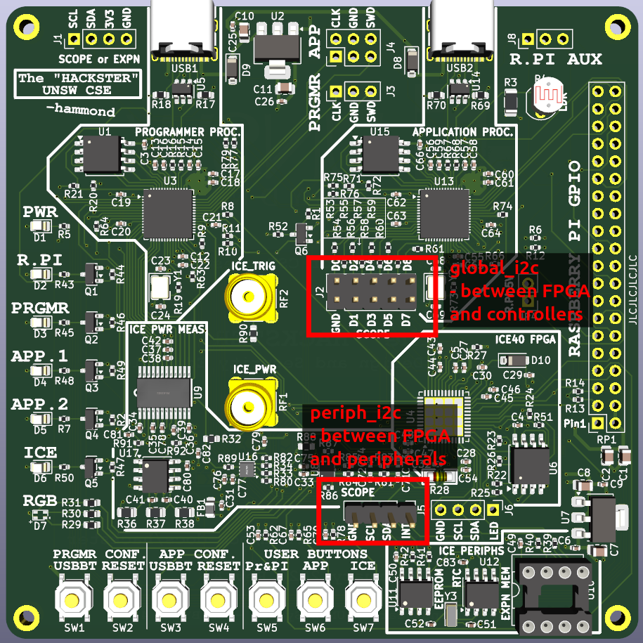
Oscilloscope connection pins
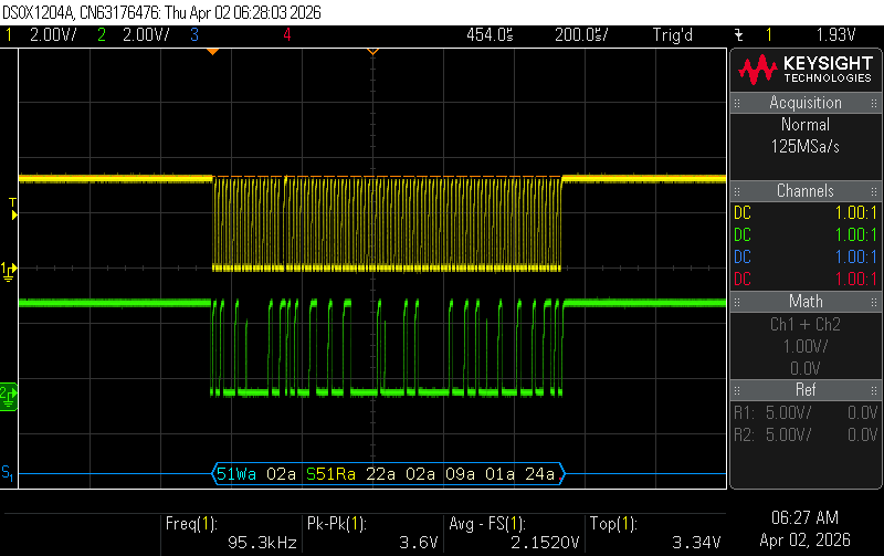
Then, if you configure the oscilloscope correctly (2V per division, 200uS per time division, trigger on falling edge of SCL, trigger mode Normal, analyze serial mode I2C with SDA as data and SCL as clock), you should be able to see the I2C transactions.
Oscilloscope connection pins
Later on, you may want to use the main J2 bus for scoping the global_i2c. You can find the pins for that using the hackster schematic.
Step 2: Interfacing the FPGA and application microcontroller with I2C
In this step, AppMicro acts as an i2c master and the FPGA is now acting as an i2c slave.
Start by copying the /examples/i2c_registers directory to your diy folder.
Now, have a look at the code, starting from the top level module registers_top in registers_top.v.
This instantiates the modules i2c_pin_primitives_ice40 and i2c_simple_slave which together provide the basic implementation of a simple read/write target at an address specified by the parameter “ice_i2c_address” (default to 0x42).
Inside i2c_simple_slave you can see the implementation of a target device mealy-type FSM alongside a few registers for storing, receiving, and transmitting data.
You should now investigate a way to implement Verilog which can control the I2C slave received/texted data such that the microcontroller can read from the button and write to RGB lights.
-
In
i2c_registers_top.v, we provided some starter code to text ICE button value to the microcontroller. Under the TODO section, fill in the logic to wire the least three significant bits of received data with RGB. The order of RGB doesn’t matter. -
Run
make run_fpgato synthesize and download it to your Hackster. -
You can run the provided
i2c_registers.micropython.pyto test your hardware. Or you can write your own micropython script to debug and verify your hardware. Consider what it is you are accomplishing here - you have an I2C master (the microcontroller) talking to an I2C slave (the FPGA), and you are controlling the slave’s behavior by sending it data. You can also use the oscilloscope to observe the I2C transactions and verify that the data is being sent and received correctly. -
When it is working, you can proceed!
Step 3: Interfacing the FPGA and RTC with I2C
In this step, the FPGA acts as an I2C master and the RTC as an I2C slave.
For this step, we will be using the i2c_master_write_rtc example as a starting point.
There are two important files in this folder.
The first is i2c_write_rtc.v, which is the top file for the project.
This instantiates an i2c master, stored in i2c_master.v, which implements a basic I2C master which can be used to read and write data to a target slave device.
In this example, however, we just write data to the RTC, and we do not read any data back.
The i2c_pin_primitives_ice40.v module is also important, as it provides the bidirectional I/O primitives for the SCL and SDA lines.
A pulldown control signal is used as the output, as with I2C, the output can either be high impedance or logic 0 (low).
An I2C master toggles the pulldown signal to indicate a 0 or Z to a connected I2C slave.
Due to the pull-up resistor on the bus, when a ‘Z’ is emitted, the bus goes to logic 1 (high).
-
Start by running
make run_fpgato synthesize and download the provided code to your Hackster. Now, press the ICE_BTN. The blue LED should go out, and the ICE LED should go on. This indicates that the example code has moved through its state machine and has activated the RTC’s timer. -
After 1 minute, the ICE LED should go out, indicating that the RTC’s timer has reached zero.
-
Re-run this example and verify with the oscilloscope that the I2C transactions are being sent correctly. You should see the I2C transaction where the master (FPGA) writes to the RTC.
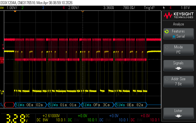
Oscilloscope capture of FPGA writing to RTC
- Copy the project to your
/diydirectory and modifyi2c_write_rtc.vto read and write different multi-byte data to the RTC. Try and recreate the behaviour from Step 1, where you set the initial time to your birthday and then read it back after a few seconds to see if it is evolving correctly. To get the output, you can emit to the RGB lights on the Hackster, or you can use the oscilloscope to observe the I2C transactions and verify that the data is being sent and received correctly.
Hint: You will need a simple FSM to switch between one write and one read operation. The existing FSM in i2c_write_rtc.v can be used as a starting point, but you will need to modify it to include the read operation. Look at the testbench file i2c_master_tb.v for an example of how to implement a read operation using the I/O of the i2c_master.v module.
Step 4: Implementing a hardware Trojan
The final step is to bring everything together and implement a hardware Trojan which can interpose on the I2C communication between the microcontroller and the RTC.
Your goal is to implement a hardware module on the FPGA that captures the signals passing through the I2C bus and modifies them in a way that allows you to change the behavior of the RTC without being detected by the microcontroller. For instance, you could implement a Trojan that intercepts the I2C communication and modifies the time data being sent to the microcontroller, causing it to read an incorrect time from the RTC.
To achieve this, you can start from the code you wrote in Step 3, and change the build (from the Makescript) to use the i2c_trojan_rtc.v file. You’ll need to instantiate both an I2C slave (which will communicate with the AppMicro) and an I2C master (which will communicate with the RTC).
Between them, you will need to encode logic: the slave will receive commands from the AppMicro, and the master will forward those commands to the RTC when appropriate.
However, in between, you can also choose to have your logic to modify the data being sent to or received from the RTC - by tactically manipulating the clock line, you can create a hardware Trojan that can edit the data to and from the RTC without being detected by the AppMicro.
This is depicted here:
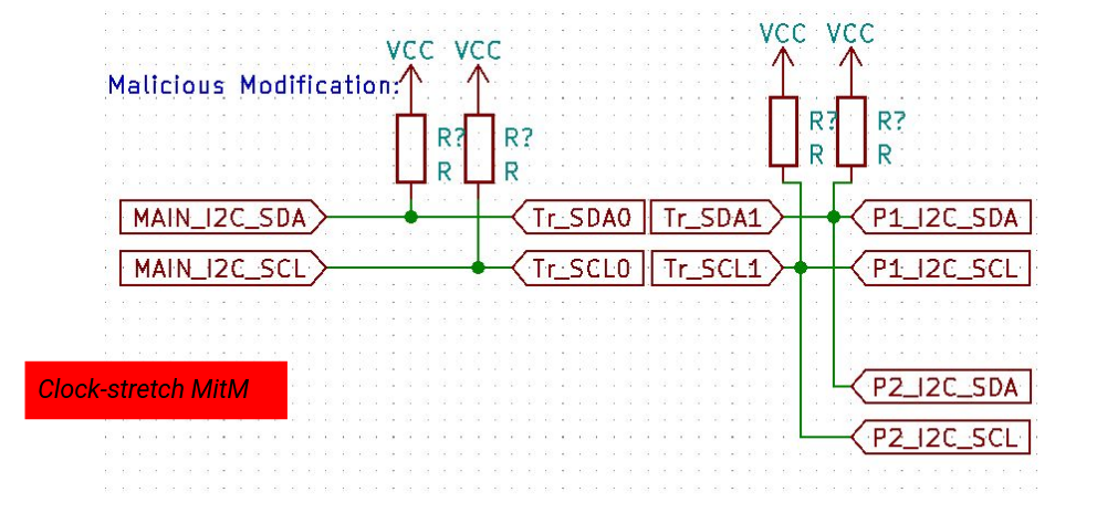
Block diagram of the I2C machine-in-the-middle attack
Multiple editing strategies are possible, and you can choose the method that you think is best. For instance, you could create a Trojan which selectively edits bytes using clock-stretching, which is a technique where the slave device holds the clock line low to delay the master from sending or receiving data. By doing this, you can create a window of opportunity to modify the data being sent to or received from the RTC without being detected.
Another method could be to implement a Trojan which simply emits modified data to the master, completely disconnecting the RTC from the communication. This would be a more simple method, but it may be less reliable / stealthy than the clock-stretching method, and the master may be able to detect that the RTC is not responding correctly.
Once you have implemented your strategy, you will be able to start thinking about how your implementation could be modified to impact the overall CTF, which has the Raspberry Pi as the main device (rather than the AppMicro), while keeping the RTC as a peripheral. Here, the RPi starts a 2 minute timer, both polling the RTC for the time and also running a GPIO trigger. Once your Trojan is reliably implemented, could you modify the FPGA bitstream to feature your Trojan, such that when the RPi tries to read the time from the RTC, it receives a modified value which causes it to miscalculate the time remaining until self-destruction?
Other methods for completing the CTF
While we’ve stepped you through the process of creating a Machine-in-the-Middle Trojan, other, more simple (and unreliable) attacks are possible (but may result in fewer marks when graded if they are excessively simple).
If you are stuck, consider using one of the other methods, which include using the FPGA to imitate the RTC without forwarding signals (i.e. an extension of just Step 2 of the walkthrough), or using the AppMicro to interfere with the RTC via its own I2C connection.